-
TEL : +886-4-2534-7800
FAX : +886-4-2534-8869
-
CELL : +886-922-111-308
Company ID:24829839
TEL : +886-4-2534-7800
FAX : +886-4-2534-8869
CELL : +886-922-111-308
Company ID:24829839
.png)
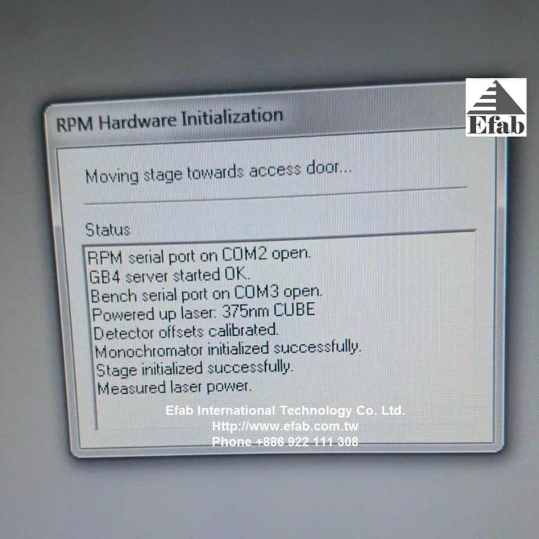
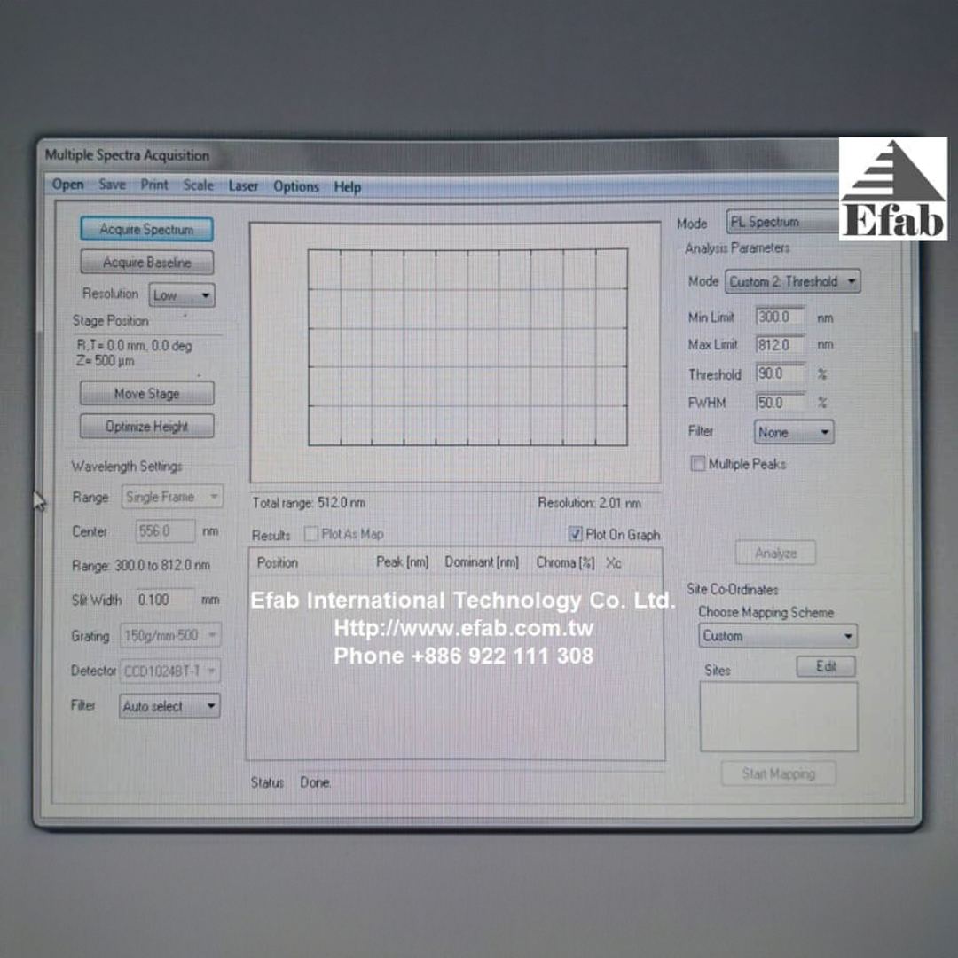
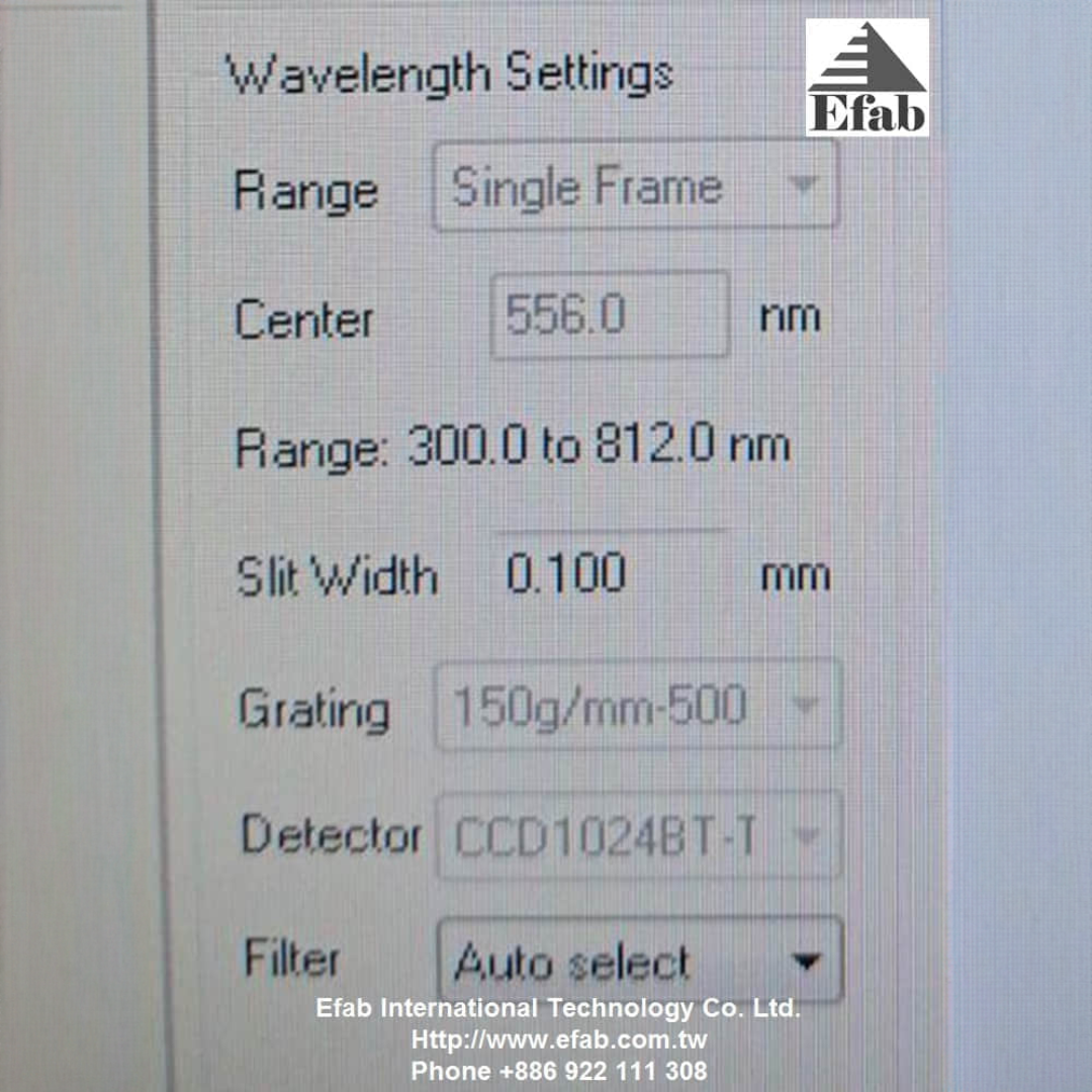
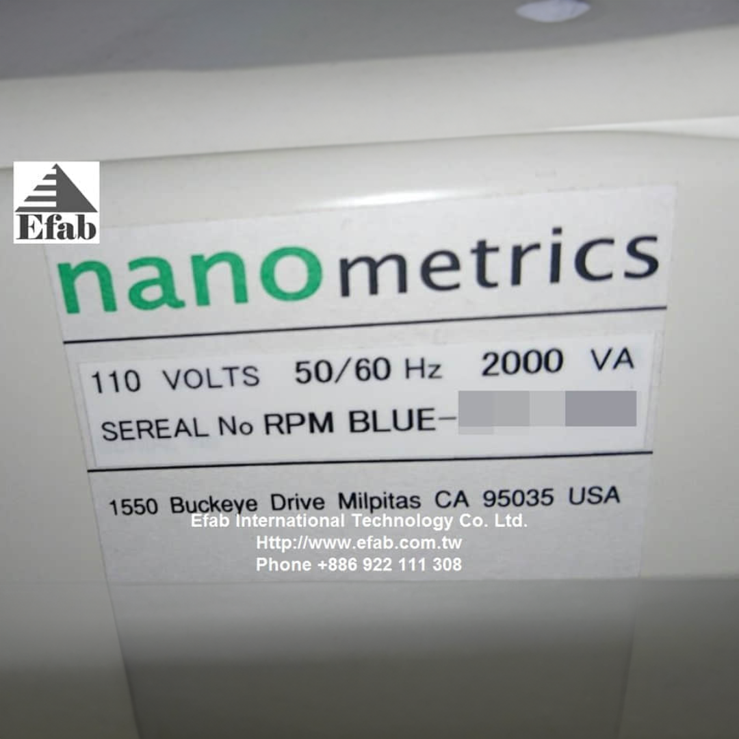
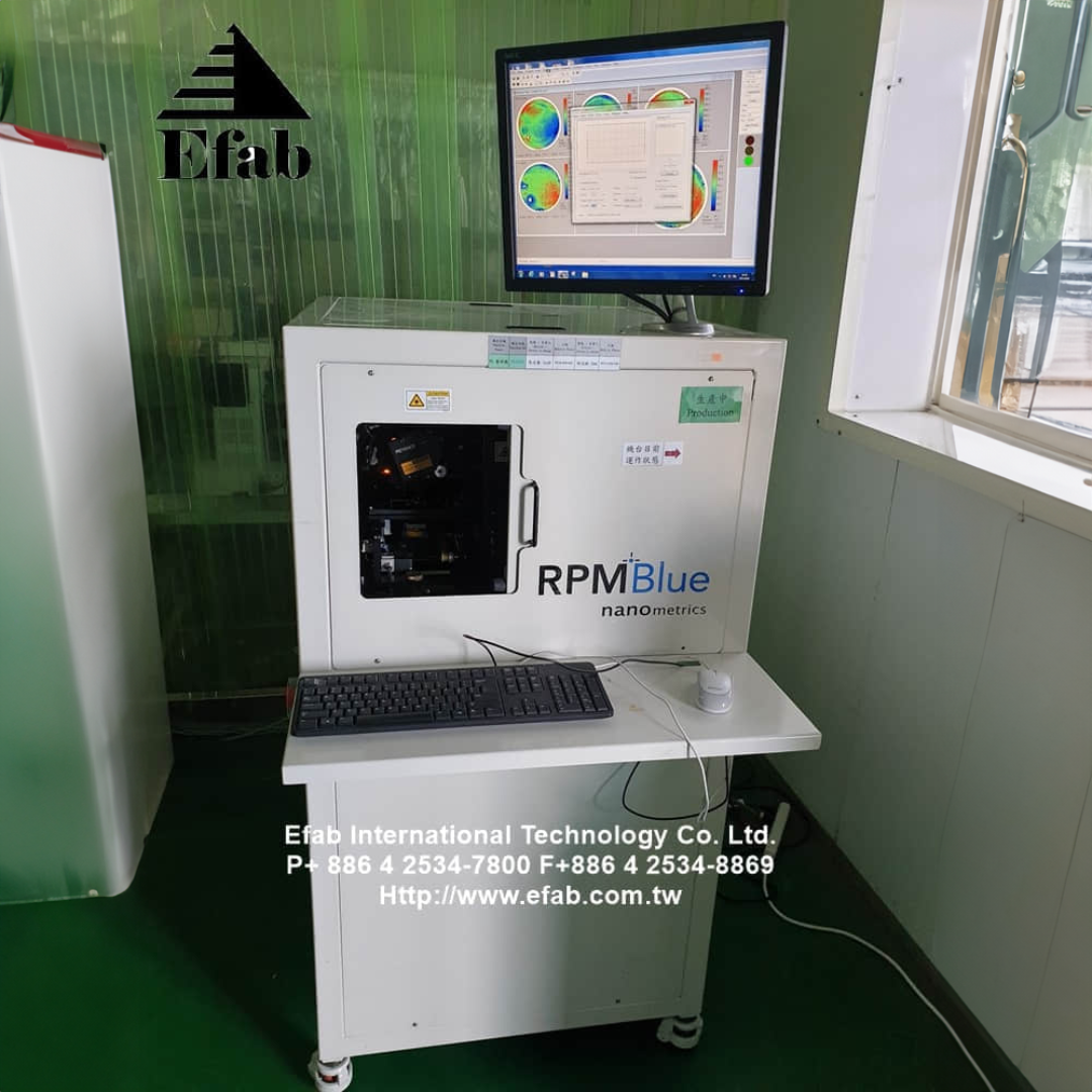
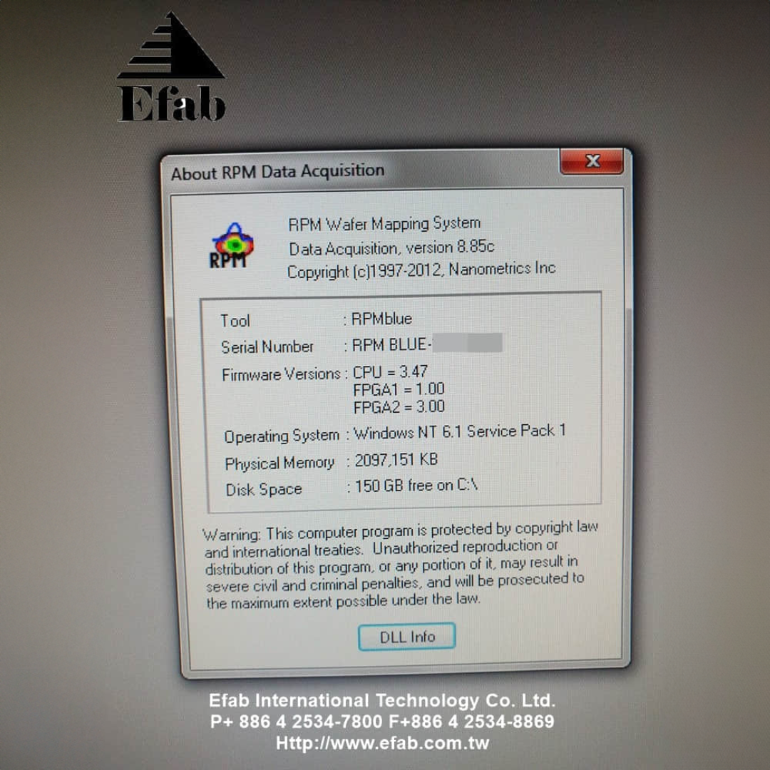
Nanometric RPMBlue Photoluminescence (PL) Mapping Tool
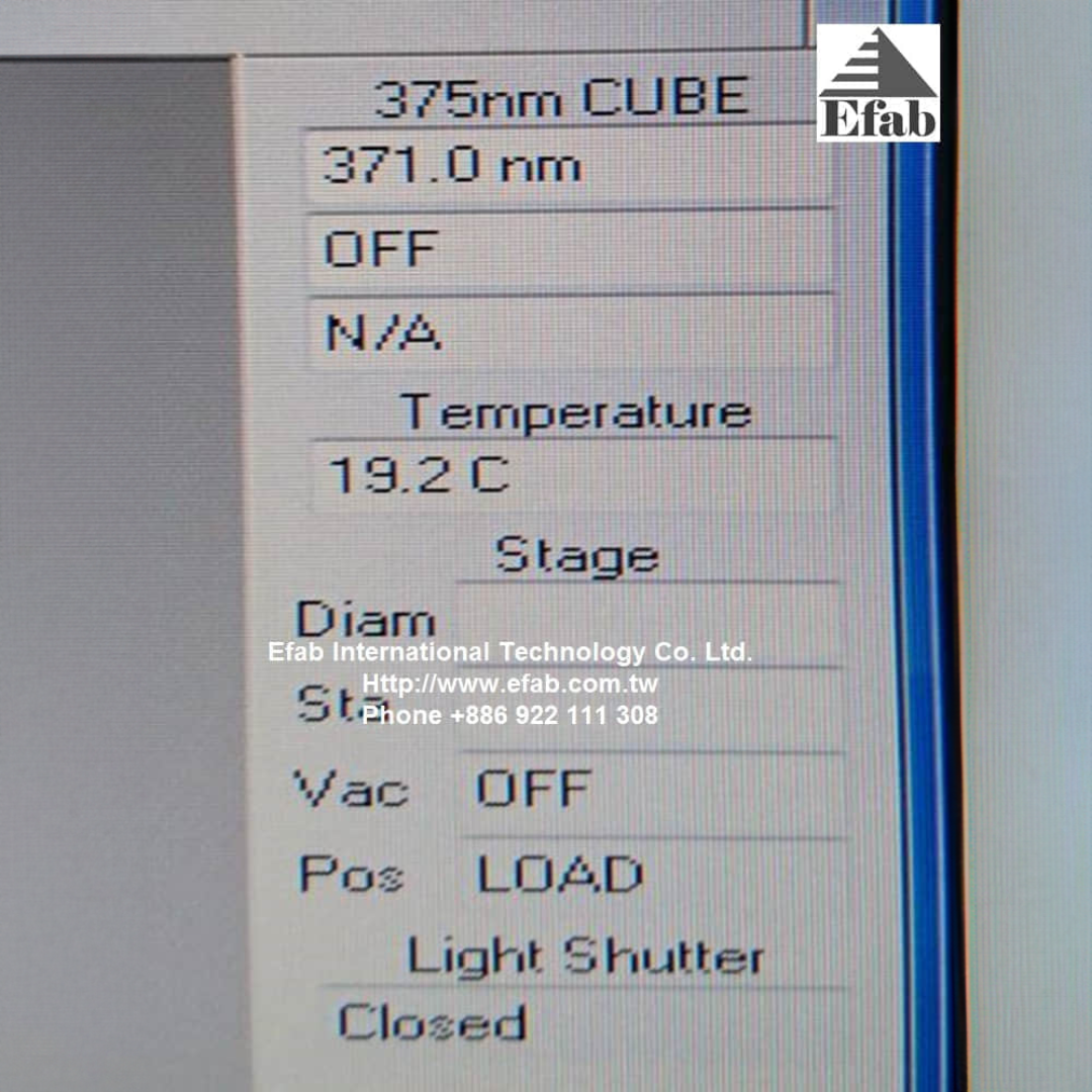
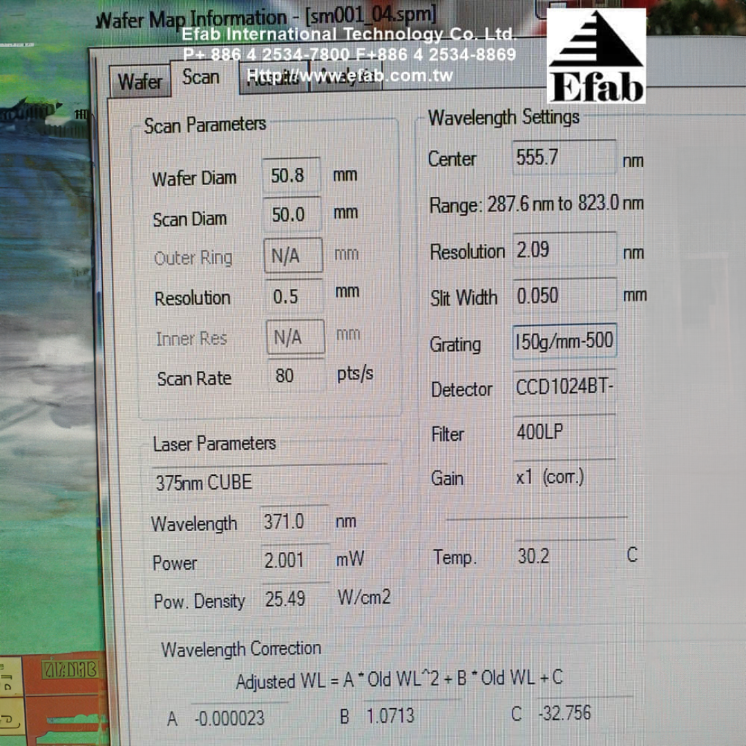
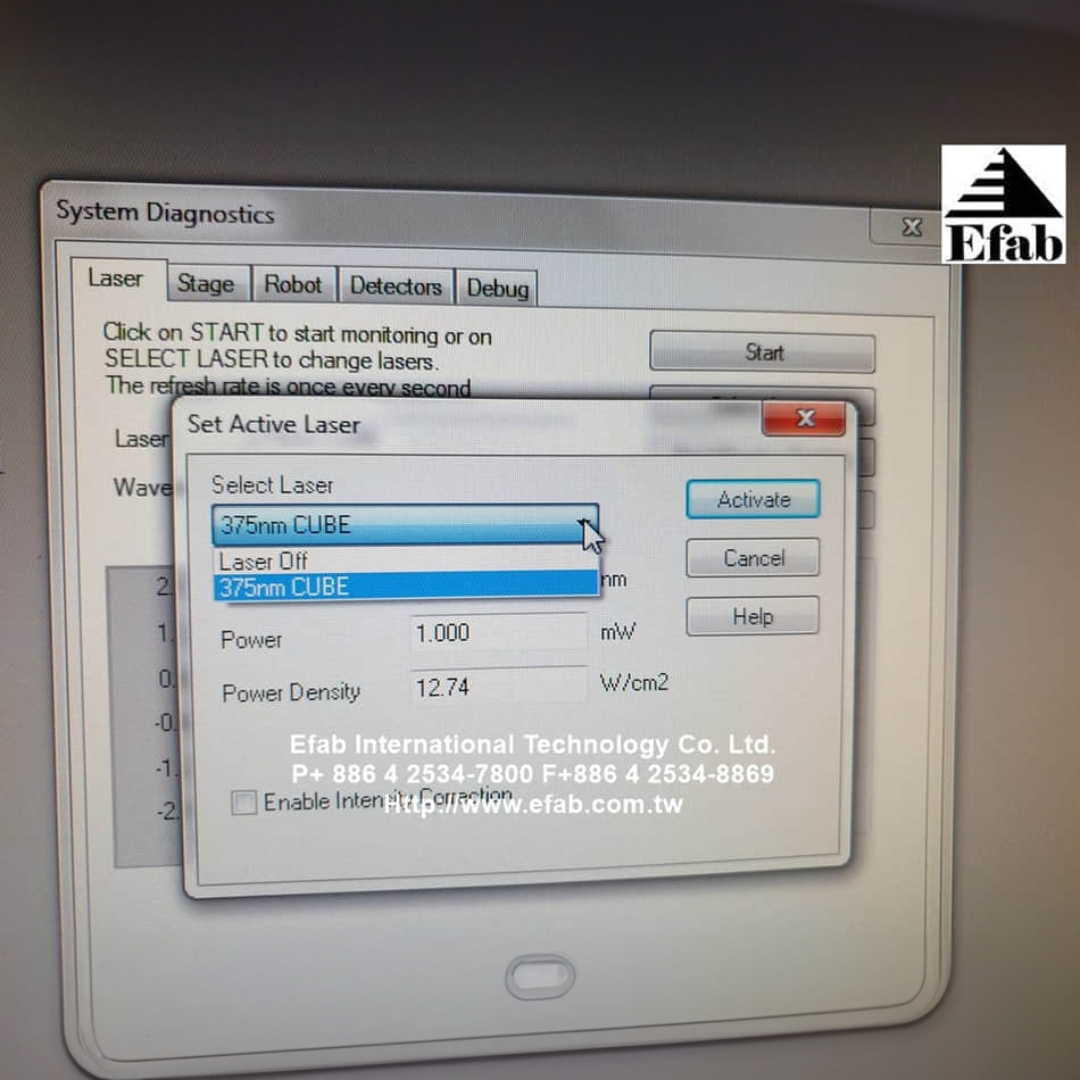
Laser : 375 nm
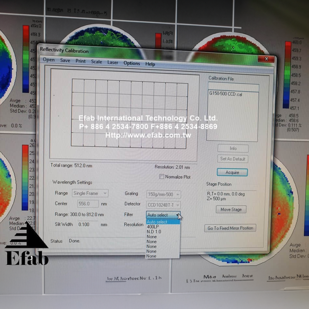
Grating : 150g/mm-500
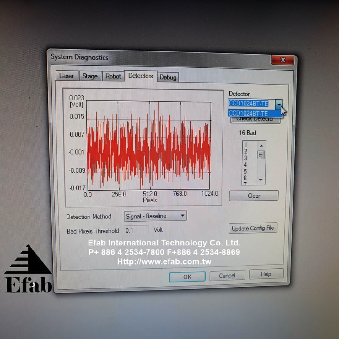
Detector : CCD1024BT - Si
The RPMBlue is the industry standard high-volume, production oriented photoluminescence mapping system. By tuning the system capabilities to your control and measurement needs for the production line, the system becomes fast and economical.
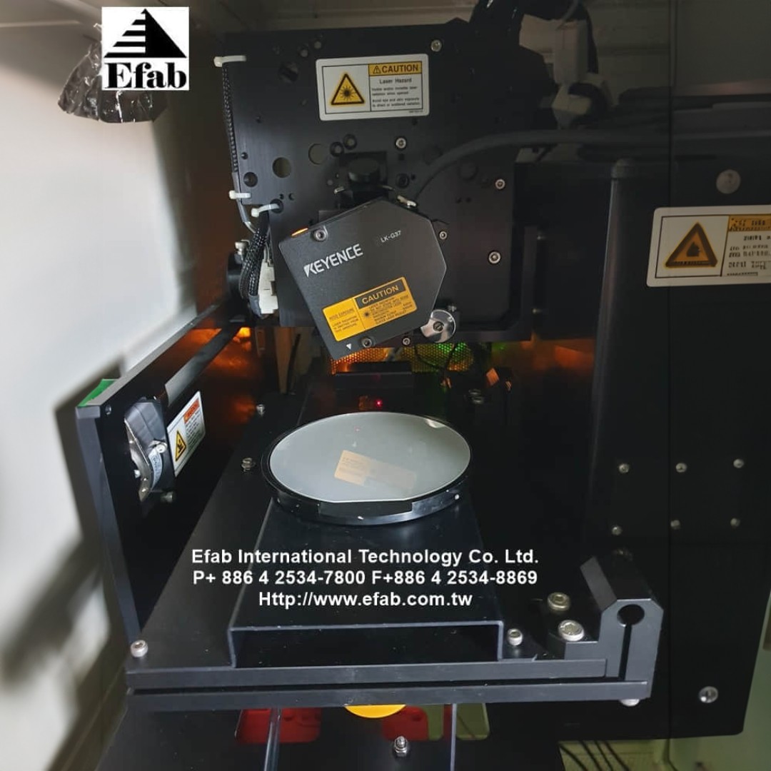
It can be fitted with up to two internal and one external excitation lasers, which are typically selected according to the bandgap of your material. Three different gratings are available to match the PL wavelength and thickness fringe range. It accommodates 2” to 6” diameter wafers standard. Certain 8” wafers can be loaded as well. Robotic loading from up to 3 cassette stations is a standard option.
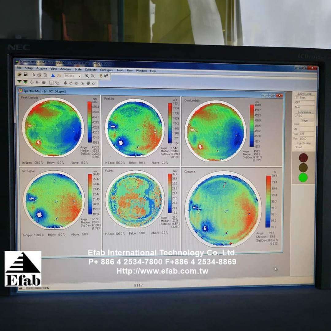
Typical applications are peak and dominant wavelength, FWHM, PL intensity, film thickness, and surface roughness monitoring of LED, Laser, high power / high frequency device epi-structures, and many other applications based on compound semiconductors.
More information available on request.